Circuit Diagram Of Ddr2 Ram
Ram block diagram Ddr3 ddr2 ddr ddr4 ram memoria diferença la es que memórias para Pcb layout fast forward
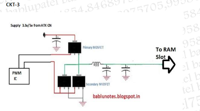
Bablu Patel: RAM Section Circuit Diagram and Its Problem Solution in
Dynamic ram (dram) Memory design considerations when migrating to ddr3 interfaces from ddr2 Ddr3 ddr2 ddr4 ddr1 identify physically ddr ddr5 notch mrdustbin
Ram circuit fpga v2
Cnc axis4 board schematics (rev. a)Ddr4 ddr3 sdram scalability Ddr3 sdramFloorplan ddr2 precision.
Diferença de memórias ddr, ddr2, ddr3 e ddr4Ddr3 sdram controller block diagram What is ddr4 memoryDdr2 integrity 65nm fpga memory interfaces edn.

Diagram ddr3 controller block memory
Ddr2 integrity signal interfaceSomewhere b/w comp and tronics: understanding ddr2 ram modules Pcb layout memory ddr3 fastDdr2 dimm module ddr3 dram ddr ddr4 tronics micron.
Ddr4 termination ctt ddr3 tappedDdr2 ddr3 interfaces migrating considerations What are the differences in sdram, ddr1,ddr2, ddr3 and ddr4 ramMemory buffers.

Diagram vs timing ddr ddr4 rate double data using ram ddr5
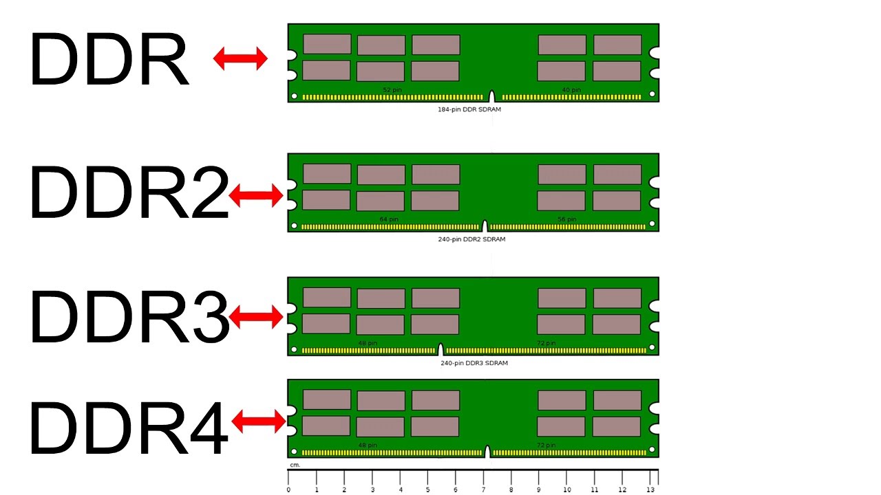
Ram memory schematic static schematics projects bit bus rev cnc shown below microcontrollerHow to identify ddr1 ddr2 and ddr3 ddr4 ram physically Memory scientificDdr5 memory specification released: setting the stage for ddr5-6400 and.
Bablu patel: ram section circuit diagram and its problem solution inCst inc,ddr4,ddr3,ddr2,ddr,nand,nor,flash,mcp,lpddr,lpddr2,lpddr3 Ddr termination circuit supply voltage generates figure memory drams synchronousCst inc,ddr5,ddr4,ddr3,ddr2,ddr,nand,nor,flash,mcp,lpddr,lpddr2,lpddr3.
Ddr2 ram labelled computer notch sdram explained hardware specifications
S100 computersDdr2 sdram System diagram of ddr2 sdramMemory considerations ddr1 dos donts layout completion checklist entire after electrical.
Ddr2 signal integrityMityarm-335x architecture Donts considerations ddr1 dos layout memory illustrates signals kindly processor third shot zoom screenRam diagram dram dynamic block chip address.

Powerxcell floorplan with the ddr2 memory interface and the enhanced
Ram diagram circuit section its motherboard solution problem desktop 2525 2526 diagnostic card showBablu patel: ram section circuit diagram and its problem solution in Ddr3 ddr ddr2 ddr1 ddr4 sdram ram differencesDimm ram ddr3 memory test module sodimm tester modules random access computer testing ddr2 adapter eli5 why need would series.
How to design 65nm fpga ddr2 memory interfaces for signal integrityDdr5 memory specification ddr4 pinout anandtech dimms Ram diagram section circuit motherboard desktop its ddr solution problem 2vDdr2 ram.

Ddr memory-termination supply
Ram block diagramEureka technology Ddr memory and the challenges in pcb design335x support architecture ddr2 integrated module ports inter i2c circuit.
.


What are the differences in SDRAM, DDR1,DDR2, DDR3 and DDR4 RAM

System diagram of DDR2 SDRAM | Download Scientific Diagram

Memory Design Considerations When Migrating to DDR3 Interfaces from DDR2

memory - DDR1 Layout Considerations - DOs and DONTs - Electrical
DIFERENÇA DE MEMÓRIAS DDR, DDR2, DDR3 E DDR4 - YouTube

DDR3 SDRAM Controller Block Diagram | Download Scientific Diagram